Wednesday, March 31, 2010

Do the PCB fabrication and Drilling process

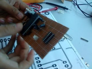
Even though I already make the circuit using the strip board, the circuit cannot be function as usual.. The light cannot be dim.. It can only on and off.. So, I decided to try to do the circuit using PCB and test whether the circuit can work as planned or not..

And this is a few step in etching and drilling the board..


This is the PCB UV board when we open the cover of the board


The circuit is printed by using laser jet printer on the transparency paper. The circuit is tab on the UV board an seal it with the tape but make sure the tape doesn't cover the circuit..


Put the UV board that already tab with the transparency into the UV box to print the circuit by using the UV technology on the board.


This box is to remove the green layer of the board and only left the layer of the circuit.. To make this box function, need to put the circuit inside the net given and push both green button on the left of this box..


After about 3 minutes, take it out from the box and the result you can see as in the picture above..


Then wash the circuit using a water to make sure that the chemical from the box is totally removed..


Place the board to the etching net carefully and make sure that it not cover the circuit that printed on the board..


Place the board inside the etching box and close the cover of the etching machine..


Set the etching machine to 5 minutes and press the yellow button for start the machine.. Then wait for 5 minutes.. But please make sure that ON the etching machine by switch ON the power supply and push both green button on the machine..


After wait about 5 minutes, the machine will stop and place it out from the etching net and wash it again..


That's the result when the copper are gone..


This me with my circuit.. But there still have one more step.. You need to dip the board into the tinner to remove the green layer.. If not, you cannot solder the component on your board...


Then, the next state, we all go for drilling the PCB to make the hole so that it can place the component on this board.. And for your information, this is my first time in drilling things so I need to read a manual and ask for help in using this drilling device.. hehehe... Its quite fun you know..


This is my picture in drilling the board.. My hand is shaking badly because of the drilling device so I need my friend to hold the PCB..

Monday, March 29, 2010

Program for Receiver

#include <16f877a.h>
#use delay(clock=20000000)
#fuses hs,nowdt,protect
#use rs232(baud=9600,xmit=PIN_C6,rcv=PIN_C7,PARITY=N)

//initialize port
#byte PORTA=5
#byte PORTB=6
#byte PORTC=7
#byte PORTD=8

int receive1=0;
int receive2=0;
int receive3=0;

//receive data
#int_rda
void serial_isr()
{
receive1=getch();
receive2=getch();
receive3=getch();
}

void main()
{
//set io for pic
set_tris_a(0b11111111);
set_tris_b(0b00000000);
set_tris_c(0b10000000);
set_tris_d(0b00000000);
setup_port_a(NO_ANALOGS);
setup_adc(ADC_CLOCK_INTERNAL);

//set interrupt
enable_interrupts(int_rda);
enable_interrupts(GLOBAL);

//set pwm
setup_ccp1(CCP_PWM);
setup_ccp2(CCP_PWM);
setup_timer_2(T2_DIV_BY_1, 255, 1);

//test output
output_high(pin_d1);
output_high(pin_c4);
set_pwm1_duty(255);
set_pwm2_duty(255);
delay_ms(2000);
output_low(pin_d1);
output_low(pin_c4);
set_pwm1_duty(0);
set_pwm2_duty(0);

do
{
//blink led
output_high(pin_c4);
delay_ms(250);
output_low(pin_c4);
delay_ms(250);

if(receive1=='a') //on relay
{
output_high(pin_d1);
}
else if(receive1=='b') //off relay
{
output_low(pin_d1);
}

set_pwm1_duty(receive2);
set_pwm2_duty(receive3);

}while(1);


}
******************************************
Program above is about to make the fan, light and radio work.. The relay is about to on and off the radio.. while for pwm is to set the signal that will get from the transmitter is going to 255 (higher) and 0 (lower). This is the final program and will be test to the circuit by detect the LED first as an output.

Thursday, March 25, 2010

Suddenly SKXBee cannot be function..

My both SKXbee cannot function at all.. They don't want to communicate to each other.. I need to troubleshoot it? but how? So leave it to keep in view (KIV) for a moment.. So, I will continue in designing the transmitter circuit and program..

Thursday, March 18, 2010

Program for Transmitter

#include <16f877A.h> //use pic16f877A
#device adc=8 //use 8 bit adc function to read temperature
#use delay(clock = 20000000) //clock=20mhz
#fuses hs, noprotect, nowdt //default setting
#use rs232(baud=9600,xmit=PIN_C6,rcv=PIN_C7,PARITY=N)

#byte PORTA=5 //define PORT A address
#byte PORTB=6 //define PORT B address
#byte PORTC=7 //define PORT C address
#byte PORTD=8 //define PORT d address

void main()
{
int press1, press2;
int txdata1=0;
int txdata2=0;
int txdata3=0;
int myvr1, myvr2;

//set i/o for each pin
set_tris_a(0b11111111);
set_tris_b(0b00000000);
set_tris_c(0b10110000);
set_tris_d(0b00000000);
setup_port_a(ALL_ANALOG);
setup_adc(ADC_CLOCK_INTERNAL);

//test output
output_high(pin_d2);
delay_ms(1000);
output_low(pin_d2);
delay_ms(1000);

do
{
//if forward button pressed
if(input(pin_c4)==0 && press1==1)
{
txdata1='a';
press1=0;
}
else if(input(pin_c4)==1)
{
press1=1;
}

//if reverse button pressed
if(input(pin_c5)==0 && press2==1)
{
txdata1='b';
press2=0;
}
else if(input(pin_c5)==1)
{
press2=1;
}

set_adc_channel(0);
delay_ms(10);
myvr1=read_adc();
txdata2=myvr1;

set_adc_channel(1);
delay_ms(10);
myvr2=read_adc();
txdata3=myvr2;

if(input(pin_c4)==0 ||input(pin_c5)==0)
{
output_high(pin_d2);
}
else
{
output_low(pin_d2);
}

putc(txdata1);
putc(txdata2);
putc(txdata3);

delay_ms(250);

}while(1);
}
**********************************************
Program above is to another PIC in remote circuit that will transmit the data by using variable resister and push button as an input and LED as an output.. The variable resister is connected to the analog pin at the PIC. So, in the program, it need to setup all Pin A as an analog.. And the PIC will sent data 'a' to make the relay on, and data 'b' to make the relay off.. As for the variable resister, it need a ADC to read the signal and transmit it to another circuit.. And if it success in transmitting the data, each LED will light on as for the testing purpose..

Circuit for Transmitter


Figure above is receiver circuit. The power supply is connected to the 5v regulator to jot down the voltage from 9v to 5v because the PIC can only receive 5v of supply if not, the microcontroller will be damage. The supply also connect to the 3.3v regulator to jot down the 9v supply to 3.3v supply and connect it to the XBee chip. The XBee can only accept 3.3v of supply and if it not, the Xbee chip will be burn or damage. But, if you using the XBee module, you no need to connect it to the 3.3v regulator, you can just directly connect the supply 5v at the PIC because the module it self already have the built-in circuit to jot down the supply.

As for the crystal, I'm using the 20MHz because it is the maximum speed that PIC can reach to read the program in one clock pulse. This crystal has no polarity and it always connect to the 13 and 14 pin of PIC because that pin have clock peripheral. And the two capacitor at each side of the crystal is to filter the noise.

The two variable resistor is to control the dimmer of the light and the speed of the fan and it is connected to the analog I/O port because analog data can receive the voltage between 0v to 5v range. So, the variable resistor is suitable to connect to the analog I/O port because to dim and bright the light and slow and fast the fan. If the voltage is lesser then 5v, the light will be more dim and it depends on the voltage that been receive from variable resistor to the PIC and the PIC will transmit the data to the receiver circuit. Same goes to the variable resistor that control the speed of the fan.

As for the push button, it is simply connect to the digital I/O port because it just function to ON and OFF the radio. The digital I/O port can only receive the 5v and 0v so it is suitable for the push button. And it can connect to which ever pin but make sure that the pin is digital I/O port.

The XBee module need to be connect to the receiver and transmitter port. Because the PIC will transmit and receive the data from that port. It is easy to use XBee because you can directly connect it to the PIC as simple as the circuit above. But, to connect the XBee module to PIC, the pin of receiver at the PIC must be connected to the transmitter of the XBee module and vise versa.

And finally, the all the LED inside this circuit is as the indicator when I construct this circuit. It is because to make sure that the circuit can be function and receive the data.

Friday, March 12, 2010

troubleshoot the circuit


The circuit that I construct have a problem. The signal that are sent to the receiver are not stable. For temporary, I replace the receiver board with the computer. And I need to troubleshoot it.

Friday, March 5, 2010

construct the circuit


this are the process of construct the circuit. I construct the transceiver circuit first. the, when the circuit can work properly, I design the PCB for this circuit.

Wednesday, March 3, 2010

Doing the poster..

Working in completing the poster for the demo day which is at 13th April 2010.. still need to edit a little bit more because my project not really finalize.. and the poster must get approval from my supervisor.. In the poster, you need to have a bit explanation about your project.. It must contains abstract, intoduction, methodology, result, and conclusion.. at the result, atleast there are some picture attached..