Saturday, November 7, 2009

final exam..

Temporary stop for final exam for two week..

Friday, October 9, 2009

draft oh draft..

I'm start in doing draft for chapter 1 and 2 which is introduction and literature review and . This draft is for my thesis. I need to submit this draft by week 13.

program...

i'm still in progress to make a program for this project..

Thursday, September 17, 2009

Design the circuit


Design the circuit in the proteus. All the circuit design in proteus is connected to the PIC16F877A. Then, search for the program to run the system. The PIC16F877A then will connected to the XBee using the previous circuit in previous assignment. Circuit above is about running light with different type of colour. This running light can be function at the personal room or as a sleeping light. I will add other application such as dimmer so that the user can control the dimmer of light using remote control.

Thursday, September 10, 2009

Block Diagam and Flow Chart

Block diagram of this subject

This block diagram represent the flow of circuit that is used inside the remote and at the home application such as fan, light, home ventilation, or home surveillance.


Flow chart of this project

This flow chart represent the flow the systems of this project. From this flow chart, you can design the program for this project.

Overall costing of this project


This are the estimate cost that will be used in this project. This cost planning is approved by my supervisor. For IC socket and IC programmer, I already explained in the previous post in the CCS C compiler title. It is not necessary for you to buy the IC socket and IC programmer per person if you're working in the group but this things are important if you want to learn programming by your own.

Thursday, September 3, 2009

Interface between SKXBee and Microcontroller


The PIC16F877A need to be interface with the SKXBee module or XBee chip because XBee chip design is not in the Proteus 7 Professional library. The microcontrollers that has USART peripheral only can interface with the SKXBee.
Picture above shown the schematic diagram to interface the PIC16F877A and SKXBee (XBee chip). All the connection are right. For the push button, it is depends on you whether you want it or not. This push button is a reset button, its function when you want the microcontroller to reset SKXBee during a run time.
But please remember DO NOT connect USB to SKXBee if it is connected to the microcontroller. SKXBee can only be connected either with USB cable or microcontroller.


Thursday, August 27, 2009

The Proposal

The Proposal that need to be done and to be submit next week(week 7) on Friday. The proposal is contain the introduction, problem statement, objective, methodology, resource planning, costing and conclusion. The problem statement is to state the problem occur during the project. The objective is the purpose in doing this project. The methodology is to explain the method that will be use to complete the project. It contain the software and hardware. Explain the procedure in doing the prototype, the process in installing the program and method in doing the circuit. The resource planning contain block diagram and gantt chart. The costing is explain about the estimate cost that is need to complete the project in the table format. And for the conclusion, it is to conclude about the project that need to be done.

Friday, August 21, 2009

WinPic 800

WinPic 800 is one of software needed to burn the program from the computer to the IC. You can get the WinPic 800 from this address http://www.cytron.com/. Download the WinPic 800 zip file from the internet then click at the file.

If your WinPic 800 is in the other language, click to the Idiama' that is placed on top of the WinPic 800 then select English.


At the right top of WinPic 800, select the PIC that you use for your program such as PIC 16f877A. PIC16F877a is in PIC16F category, so select PIC 16F then, at the bottom of that, select the PIC16F877A.


Then change the setting of the hardware and software that suitable to the IC that been used.

To burn the program, go to file> open. Then search the program location that you been saved. then click open. Then the WinPic will read your program. Then click program all that in the red circle in the figure below. Then the program will recognize your PIC and burn the program into the PIC.

Thursday, August 20, 2009

CCS C Compiler

CCS C compiler features

The CCS C compiler supports the microchip PIC12X. PIC16X, PIC18X and dsPIC device.


  • PCB Compiler supports PIC16C5X
  • PCM Compiler supports PIC16C6X, 7X, 77X, 8X, 8XX & 9X.
  • Built in libraries for all PICs, RS232, I/O, I2C, and delay.
  • Integrates with MPLAB and other simulators/emulators for source level debugging
  • Formatted print allows easy formatting in Hex or Dec.
  • Efficient function implementation allows call trees deeper than the hardware stack
  • Access to hardware from C functions: Timers, A/D, E2, SSP, PSP, I2C
  • 18 and 16 bit types
  • Assembly code may be inserted anywhere in source and may reference C variables
  • Automatic linking handles multiple code pages
  • Inline procedures supported to save stack space, linker automatically determines optimum architecture
  • Standard one bit type (short int) permits the compiler to generate efficient bit oriented code
  • #BIT and #BYTE allow C variables to be placed at absolute addresses to map to C variables
  • IRQ procedures supported on PCM. Start-up and clean-up code is generated
  • Updates via modem for 30 days included


The CCS C compiler is one of the C compiler that manufactured by CCS. C compiler is a computer program or set of program that transforms source code written in a computer language (C++ language) into another computer language (binary form).

When you want to use the CCS C compiler,

  1. First you have to download the CCS C Compiler.
  2. After that, double click the PIC C compiler icon on the desktop.
  3. Click at the file picture on the left top of the PCW
  4. Then open the new file by clicking new-source file.
  5. Create your own program.
  6. After your program is complete, compile the program to make sure that there is no error. If there is an error of your programmig, you have to modified your program so that, the error will gone. If not, you cannot execute the program into the PIC.

To burn your program to the IC, you have to place the IC to the IC socket and connect the IC socket to the PIC programmer. By using the WinPIC 800 software, execute the program into the PIC. The IC socket and PIC programmer is one of the cytron product. You can buy it online from this web site http://www.cytron.com.my/ or you can buy it from other electronics distributer or shops. Another product from cytron that can used to burn the program to the IC is SK40B. SK40B has more function and much easier.

UIC00A (USB ICSP PIC Programmer) UIC-S (UIC00A socket)

Proteus 7 Professional


Proteus is a low-cost EDA package offering facilities for schematic drawing, SPICE simulation, and PCB layout. The ProSPICE simulation module also includes cosimulation of the PIC16F84 microcontroller, and a range of interactive peripheral models such as LCD displays, matrix keypads, and an RS232 terminal.

Proteus is an easy-to-use application for creating printed circuit-board layouts, and is good for hobbyists or students working on small projects. Proteus creates simple PCBs with 16 copper layers, two silk screens, and four user/mechanical layers, plus an autorouter. Completed designs are suitable for reports, tutorials. or articles. Proteus is a great program for creating PCBs.


The VSM advantage

The Proteus Design Suite is wholly unique in offering the ability to co-simulate both high and low-level micro-controller code in the context of a mixed-mode SPICE circuit simulation. With this Virtual System Modelling facility, you can transform your product design cycle, reaping huge rewards in terms of reduced time to market and lower costs of development.

If one person designs both the hardware and the software then that person benefits as the hardware design may be changed just as easily as the software design. In large organisations where the two roles are seperated, the software designers can begin work as soon as the schematics is completed. There is no need for them to wait until a physical prototype exists.

In short, Proteus VSM improves efficiency, quality and flexibility throughout the design process.

Proteus Virtual System Modelling (VSM) combines mixed mode SPICE circuit simulation, animated components and microprocessor models to facilitate co-simulation of complete microcontroller based designs. For the first time ever, it is possible to develop and test such designs before a physical prototype is constructed.

This is possible because you can interact with the design using on screen indicators such as LED and LCD displays and actuators such as switches and buttons. The simulation takes place in real time (or near enough to it): a 1GMHz Pentium III can simulate a basic 8051 system clocking at over 12MHz. Proteus VSM also provides extensive debugging facilities including breakpoints, single stepping and variable display for both assembly code and high level language source.


Friday, August 14, 2009

PIC16F877A Pin Description and features


Special Microcontroller Features
- 100,000 erase/write cycle Enhanced Flash program memory typical
- Self-reprogrammable under software control
- Single-supply 5V In-Circuit Serial Programming
- Watchdog Timer (WDT) with its own on-chip RC oscillatpr
- Programmable Code Protection
- Power-Saving Sleeping mode

Peripheral Features
- Two 8-bit (TMR0, TMR2)timer/counter with Prescalar
- One 16-bit timer/counter
- Brown-out detection circuitry
- Parallel Slave Port (PSP): 40/44 pin-device only

High-Performance RISC CPU
- Only 35 single-word instructions to learn
- DC-20MHz clock input
- Up to 8K x 14 words of Flash Program Memory
- Pinout Compatible to other 28-pin or 40/44-pin

Analog Features
- 10-bit, up to 8-channel Analog-to-Digital Converter (A/D)
- Brown-out Reset(BOR)
- Two analog comparators
- Programmable on-chip voltage reference (VREF) module CMOS Technology
- Low-power, high-speed Flsh/EEPROM technology
- Fully ststic design
- Wide operating voltage range (2.0V to 5.5V)
- Low-power consumption

Sunday, August 9, 2009

Communicate between two XBee

XBee can communicate to each other using computer. There are several procedure to communicate the XBee. But, first of all, we need to check the functionality of the XBee module.This are the procedure to check the XBee module:


  1. Simply connect USB cable (B type) to SKXBee USB socket, another end (A type) to PC.

  2. Please refer to document named “USB Driver Installation Guide” for driver installation.
  3. Setup X-CTU with double-clicking the “setup_x-ctu.exe” file that can get from the SKXBee page.

  4. Launch the X-CTU Software and select the “PC Settings” tab. Verify the baud and parity settings of the COM port match those XBee Module. The virtual COM Port is normally located at the last port, USB serial Port.


  5. Choose the COM Port and click ‘Test/Query’ tab. Then, click ‘OK’.


  6. To modify or read XBee Module parameters, the module must first enter into Command Mode.

  7. First, select the ‘Terminal’ tab on X-CTU Software. To enter AT Command Mode, send the 3-character command sequence ‘+++” and XBee module will response ‘OK’ which means that it has already enter Command Mode.

  8. When a command is send to a module, the module will parse and execute the command. Upon successful execution of a command, the module returns an “OK” message. If execution of a command results in an error, module will return “ERROR” message.

  9. To exit AT Command Mode, send ATCN Command or if no valid AT Command are received within the time specified by CT (Command Mode Timeout) Command, the XBee Module automatically returns to Idle Mode. So, if another command need to send, ‘+++’ should be enter so that module will enter into Command Mode again.


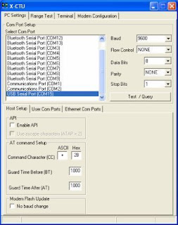
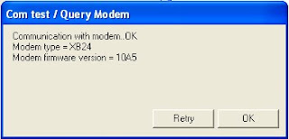
To communicate between two SKXBee:

  1. Connect two SKXBee with two different computer.

  2. Then, do the procedure above at both computer to check the functionality of both SKXBee.

  3. Let name one SKXBee with SKXBee1 and onother one with SKXBee2.

  4. Source Address (MY) of SKXBee1 must be match to Destination Address (DL) of SKXBee2 and Destination Address (DL) of SKXBee1 must be match to Source Address (MY) of SKXBee2.
  5. After built connection between these two SKXBee, they can communicate among each other. Data sent by SKXBee1 will received by SKXBee2 and data sent by SKXBee2 will
    received by SKXBee1.

  6. Data which is sent is in blue color and data which is received is in red color. Below is example of data sent and received of SKXBee1 and SKXBee2 in X-CTU terminal.

Tuesday, August 4, 2009

ZigBee Application

ZigBee is a standard for wireless data transmission just like Wi-Fi and Bluetooth. The entire device (wireless device) is function to move the desired data to the next carrier in the communications path until the data is delivered to the target end-point.

MaxStream is a well-known manufacturer of components for wireless communication. ZigBee is one of the MaxStream products. There are two versions of ZigBee that are available from MaxStream which are XBee and XBee PRO. Both versions are functionally identical and pin compatible. The only difference is the transmit power, which is 1mW maximum for XBee and 63mW maximum for XBee PRO. ZigBee’s mission is to cut the traditional wires between sensors, wired slaves devices, and the microcontrollers and microprocessors they serve.


ZigBee is available in three difference antenna:-
1. Integrated into the chip. In this case the radiated energy is practically non-directional
2. With an antenna connector for attaching an external antenna.
3. With an integrated vertical (whip) antenna.

ZigBee can be interfaced quite easily via a standard serial port, such is commonly found in the microcontrollers (UART) or the COM port of a PC (RS232), at maximum rate baud of 115, 200. The XBee is powered from a 3.3v supply instead of 5v supply like most digital circuits.


AT command structure. XBee modules recognize such command.


The commands are actually just ASCII codes (character strings). You send commands to the XBee the same way as data, and there is a bit of software that tells the two apart. This works as follows. Before send a command, you have to put the XBee in the ‘wait for command’ state. To do so, you send it a string of three + characters (hex 2B), or literally ‘+++’. After this, the XBee expects to receive a command in Hayes format, which always starts with ‘AT’ (which stands for ‘attention’) in ASCII code, followed immediately by the actual command and any command parameters that may be necessary. The command string is terminated by a Carriage Return (CR) character. Figure above shows an example of all this. The XBee module executes the command and then reports whether the command was processed successfully. If everything went the way it should, the XBee returns ‘OK’, while otherwise you will receive an error string from the module.


Internal block diagram of the XBee


A wireless link is always half-duplex. It can transmit or receive with a single antenna, but not both at the same time. However, your application can transmit and receive at the same time (full-duplex mode) via a serial link to the UART at your end of the interface. Data is presented to the XBee module through its DIN pin, and it must be in the asynchronous serial format, which consists of a start bit, 8 data bits, and a stop bit. Because the input data goes directly into the input of a UART within the XBee module, no bit inversions are necessary within the asynchronous serial data stream. All of the required timing and parity checking is automatically taken care of by the XBee’s UART. This is made possible by two software buffers. The principle is revealed in figure above. As you would expect, the XBee module produces a received data asynchronous serial data stream for the host on its DOUT pin. So, all you need is a simple three wire (DIN, DOUT, and ground) serial connection to put ZigBee to work with the XBee and XBee-Pro modules.

There is a transmit buffer and a receive buffer, and each buffer provides a temporary parking place for 100 bytes. Data can arrive from both directions at the same time – the data to be transmitted coming from the UART, and the data received by the antenna from the RF link. When the antenna is receiving data, it cannot transmit data at the same time. For this reason, the data to be transmitted is parked in the transmit buffer for a while, and the received data is stacked up in the receive buffer. As soon as the data stream from the RF end stops, the XBee module switches the antenna from receive to transmit and empties the transmit buffer by sending its content out on the ether. At the same time, the UART empties the receive buffer by sending the data in it to your application. An application with a large amount of data to send can easily overload the transmit buffer. MaxStream provides a ‘full’ alarm to deal with this problem. As soon as the application has filled all but the last 17 bytes of the transmit buffer (which means 83 bytes are waiting to be transmitted), pin 12 goes high to signal to the system that it has to stop filling the buffer for a while. Pin 12 goes low again after the content of the transmit buffer has been reduced to 66 bytes. This can be regarded as a sort of software hysteresis.


Pin description of the XBee chip.

Figure above shows the internal block diagram of the XBee module, which forms the core of a specific application. The XBee module has 20 leads, which is same with the DIL packages used for digital ICs. But, due to the very compact dimensions of the module, the pins are separated by only 2 millimetres, so they won’t fit in an IC socket. Fortunately for anyone who wants to keep the module replaceable, suitable PCB connectors are available from Radiospares under item number 131.9872 (they are often used in PC mice). For good measure, would like to remind again that the maximum supply voltage is 3.3 V. anything more than this will unavoidably result in the premature death of your treasured module.

The supply voltage must be decoupled by a 100-nF capacitor located as close as possible to pins 1 and 10. Communication is provided by pins 2 and 3, and the direction is indicated by arrows. Some of the pins are marked with an asterisk (*). These pins are reserved for certain functions that are not yet available from the manufacturer. When they are available, it can download from the MaxStream website and upgrade the XBee by flashing the firmware into the module. Up until then, simply leave them unconnected. The same applies to the pins marked NC (‘not connected’). Pin 5 is more important: logic 1 here (3.3 V) enables the module, while logic 0 disables it. A 10-k_ pull-up resistor from pin 5 to pin 1 ensures that the module will be enabled as soon as the supply voltage is applied. You have a choice of several functions for pin 9. An internal parameter determines which of them is active. The most important function is the sleep state. The module remains in deep sleep as long as the internal SM register is not at logic 0. Pin 7 provides a pulse-width modulated (PWM) signal proportional to the most recently received RF signal. It has a period of 8.32 ms, which corresponds to 120 Hz. Fans of LED bars and other light effects can convert it into an analogue signal and use it as a signal strength indicator (all you need is an RC network and an LM3914). This can also be done using software, since the strength of the most recently received signal is stored in the internal DB parameter.